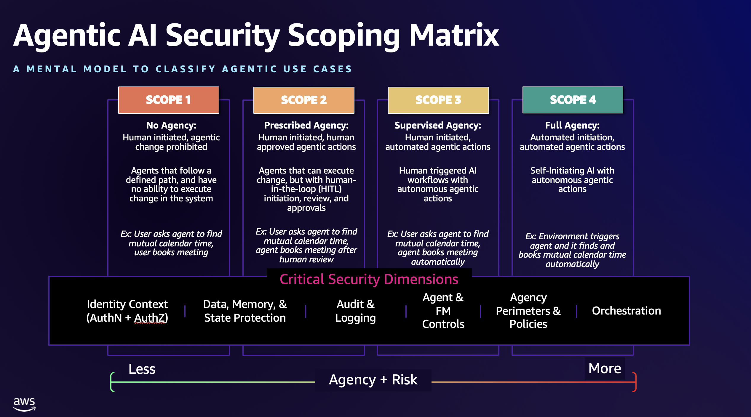
The traditional dependence on the Central Processing Unit (CPU) as the primary engine for silicon-based intelligence has reached a thermal and logic-gate bottleneck. As Moore’s Law transitions from a predictable scaling of transistors to a desperate scramble for architectural efficiency, the industry has shifted toward Domain-Specific Accelerators (DSAs). The most significant of these is the Neural Processing Unit (NPU). Understanding the NPU requires moving past the marketing jargon of "AI-enabled PCs" and dissecting the mathematical necessity of tensor-based computation over scalar or vector processing.
The Mathematical Divergence of NPU Architecture
To grasp why the NPU is replacing the GPU and CPU for specific workloads, one must analyze the data types and movement patterns inherent in deep learning. CPUs are designed for low-latency, complex branching logic. They excel at "if-then-else" scenarios. GPUs are throughput-oriented, handling thousands of parallel threads for vertex shading and pixel manipulation. However, transformer-based models and large language models (LLMs) rely almost exclusively on massive matrix-matrix multiplications ($C = A \times B$).
An NPU is fundamentally a spatial array of Processing Elements (PEs). Unlike a CPU, which fetches an instruction, decodes it, and executes it on data from a cache, an NPU often employs a systolic array architecture.
In a systolic array, data flows through the network of PEs like blood through a circulatory system. The weights of a neural network layer are pre-loaded into the PEs, and the input data moves across the rows and columns. This minimizes "data movement," which is the primary source of energy consumption in modern computing. The energy cost of moving data from off-chip DRAM to the processor can be 1,000 times higher than the cost of the actual floating-point operation. By keeping data local to the execution units, the NPU achieves an orders-of-magnitude increase in Performance-per-Watt.
The Three Pillars of NPU Efficiency
The superiority of the NPU is not derived from raw clock speed—many NPUs run at significantly lower frequencies than high-end CPUs—but from three structural advantages.
1. Reduced Precision Arithmetic
While scientific simulations require 64-bit double-precision floats (FP64), neural networks are remarkably resilient to "noise." The NPU leverages this by utilizing lower-precision formats such as INT8, FP16, or the more recent BF16 and FP8. Reducing precision from 32-bit to 8-bit cuts the memory bandwidth requirement by a factor of four and the silicon area for multipliers by even more. This allows for higher density of arithmetic logic units (ALUs) within the same thermal envelope.
2. Zero-Shedding and Sparsity Hardware
Neural networks are often "sparse," meaning many of the weights or activations are zero. A general-purpose CPU still spends cycles multiplying by zero. Modern NPUs include dedicated hardware to detect and skip zero-valued operands. This "sparsity acceleration" allows the chip to claim effective TOPS (Tera Operations Per Second) that far exceed its physical raw throughput by only performing meaningful calculations.
3. Scratchpad Memory vs. Hierarchical Cache
CPUs use complex L1/L2/L3 cache hierarchies managed by hardware logic to guess what data the processor will need next. NPUs typically use a software-managed "scratchpad" memory. Because the data flow of a neural network inference pass is deterministic—the weights and the sequence of operations are known before the first bit is processed—the compiler can explicitly schedule every data move. This eliminates the silicon overhead of cache controllers and the energy waste of cache misses.
The Latency vs. Throughput Trade-off
A critical misunderstanding in current technology analysis is the conflation of GPU "throughput" with NPU "efficiency." When running an LLM locally on a mobile device or a laptop, the bottleneck is rarely the peak TFLOPS (Tera Floating Point Operations Per Second). Instead, the bottleneck is the Memory Bandwidth Wall.
LLMs require fetching every parameter of the model from memory for every single token generated. If a model has 7 billion parameters (INT8), it requires 7GB of memory bandwidth per token. At a generation speed of 10 tokens per second, the system needs 70GB/s of sustained bandwidth.
- GPUs address this with massive, power-hungry wide memory buses (GDDR6/HBM).
- NPUs address this by integrating more closely with the System-on-Chip (SoC) and utilizing aggressive compression algorithms to minimize the data footprint.
This creates a structural divide: GPUs remain the kings of "training" (massive throughput, high power), while NPUs are the undisputed masters of "inference" (low latency, high efficiency, constrained power).
The Software Stack Bottleneck
The hardware capability of an NPU is irrelevant without a robust compiler and abstraction layer. This is where the industry currently faces its greatest fragmentation. Unlike the CPU world, which has standardized around x86 and ARM, or the GPU world, dominated by NVIDIA’s CUDA, the NPU ecosystem is fractured.
Each vendor—Qualcomm with the Hexagon, Apple with the Neural Engine, and Intel with the NPU integrated into Core Ultra—uses proprietary drivers and intermediate representations. Developers are forced to use frameworks like ONNX Runtime, OpenVINO, or CoreML to bridge the gap. The "Tax of Translation" often negates the hardware speed advantages if the compiler cannot effectively map the neural network graph to the specific PE layout of the silicon.
The Cost Function of Integration
Integrating an NPU into a standard processor design involves a significant "Area Tax." Every square millimeter of silicon dedicated to the NPU is space taken away from the CPU’s cache or the GPU’s execution units.
The strategic decision for silicon designers is no longer "should we include an NPU," but "how much of the die should it occupy?" Current trends suggest a 15% to 25% allocation of die area to neural acceleration in flagship mobile SoCs. This investment is justified by the offloading of tasks such as:
- Computational photography (ISP integration).
- Real-time voice-to-text and translation.
- Background noise suppression and video framing.
- On-device LLM execution for privacy-centric personal assistants.
The Myth of the "AI PC"
The marketing term "AI PC" suggests a qualitative shift in what a computer is. Rigorous analysis suggests otherwise. The AI PC is simply an architectural correction. For decades, we have used general-purpose processors to perform highly specific mathematical tasks. This was inefficient. The NPU is a return to specialized hardware, similar to how the GPU was born to handle the specific geometry of 3D graphics.
The real transformation lies in the shift from Instruction-Based Computing to Weight-Based Computing. In instruction-based systems, the logic is stored in the code. In weight-based systems, the logic is stored in the parameters of the model. The NPU is the first processor designed where the "program" is a multi-gigabyte matrix rather than a sequence of 64-bit instructions.
The Structural Limitation of NPUs
Despite their efficiency, NPUs are not a panacea. Their greatest strength—their specialization—is also their primary weakness. If a new type of neural network layer is invented (e.g., a shift from Transformers to a completely different architecture like State Space Models), a hard-wired NPU might lack the flexibility to accelerate it efficiently.
This creates a "Fixed-Function Risk." If the silicon is optimized for 3x3 convolutions but the industry moves toward large-scale attention mechanisms, the NPU becomes "dead silicon"—taking up space and adding cost without providing value. Consequently, the most successful NPU designs are those that maintain a degree of programmable VLIW (Very Long Instruction Word) capability alongside their fixed-function matrix units.
Strategic Recommendation for Implementation
For CTOs and system architects, the move toward NPU-heavy hardware necessitates a three-pronged strategy:
- Quantization-First Development: All neural assets must be optimized for INT8 or FP8 precision immediately. Developing for FP32 is now a legacy approach that will lead to thermal throttling and unacceptably high latency on edge devices.
- Abstraction Layer Neutrality: Avoid deep integration with vendor-specific NPU toolkits. Utilize cross-platform runtimes (like ONNX) to ensure that logic remains portable as the NPU hardware wars evolve over the next 36 months.
- Local vs. Cloud Load Balancing: Architect applications to recognize the "TOPS availability" of the local machine. If an NPU is present, execute privacy-sensitive or low-latency tasks (like UI-level AI) locally. Reserve the cloud for high-parameter "Reasoning" tasks that exceed the local memory bandwidth capacity.
The NPU is not a "game-changer" in the sense of a sudden miracle; it is the inevitable conclusion of the physics of power density and the mathematics of the tensor. The age of the general-purpose processor is ending, replaced by a heterogeneous era where the NPU is the primary steward of the user experience.
Would you like me to analyze the memory bandwidth limitations of specific NPU implementations like the Qualcomm Snapdragon X Elite versus the Apple M4?